Before going to know about Power Planning in ASIC designs. Let us raise a question, why do we need power planning? In fact, in higher node technologies power planning is not a big task, area, and performance were the things are more concerned while designing. But while technology got advanced (lower technology nodes), the power started dominating the area and performance. Because nowadays all devices are becoming portable, movable, and powering those devices using batteries, so small capacity batteries should last for more time while used. The best example of portable devices is TWS earbuds, smart watches, fitness bands, etc.…
The main agenda of the power plan is to create a proper way to send the power from outside of the world to the standard cells and macros through the power routes.
The flow of power or we can say levels of power distribution shown in below flow:
Power pads
⇓
Power rings
⇓
Power stripes
⇓
Power rails
⇓
Standard cells
This entire flow also termed as Power Distribution Network (PDN). Because this network delivering the power from outside world to the standard cells present inside the chip. Following figure shows an example diagram for the PDN.
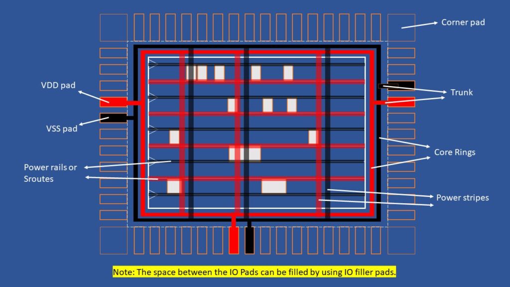
Power Pad
Power pads are placed along with IO pads in the pads section of the full chip. These pads pass the power from outside of the chip to the power rings. So, power pads act as a bridge to pass the power from the outside to the chip. (You can see the power pads in the above figure, the Red color pad indicates the VDD and the Black color pad indicates the VSS).
Trunks
Trunks are the nets that connect the power pads and the core rings.
Core rings
A set of rings creates around the core (Exactly in the area of the core to IO boundary). These rings get power from the pads and supplies to the power stripes.
Note: VDD ring + VSS ring = one core ring set
Stripes
Power stripes are flies over the core area. The power stripes on both ends connect to the core rings. Power stripes are always created in the top metal layer. And these stripes supply power from the core rings to the power rails (Sroutes).
Note: VDD + VSS = one stripe set, in the above example we can see there are 3 sets.
Power rails (Sroutes)
Power rails are connected to the power stripes using power vias. These rails are created at Metal layer 1 and vias are dropped from the top metal layer to the bottom layer. The power pins of standard cells are directly connected to the power rails which are present in layer 1 because the power pins of the standard cells are available in metal layer 1.
The following figure shows, how the power stripes and power rails are connected through the power vias. Power via drops from the top metal layer to metal 1(bottom metal layer) to connect power stripes to sroutes (wherever these two intersects).
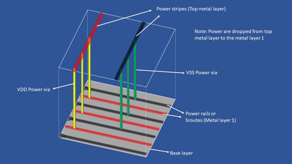
Note: Standard cells sitting in base layer and their power pins are presents at Metal layer 1
Inputs of Power plan
- Netlist
- Timing libraries
- Physical& technology libraries
- RC coefficient
- SDC
- UPF (Unified Power Format) or CPF (Common Power Format) – (if the design have multiple voltage domains)
Outputs of power plan
- Floorplan DEF with Power Distribution Network (PDN)
Things You Must Know
Do you think the above content is enough in terms of power planning? The answer is no. You should understand some of the basics of power consumption because there are some power-related issues rises in the design. Following are the types of power dissipation effects the design:
- Static power dissipation
- Dynamic power dissipation
Static power dissipation
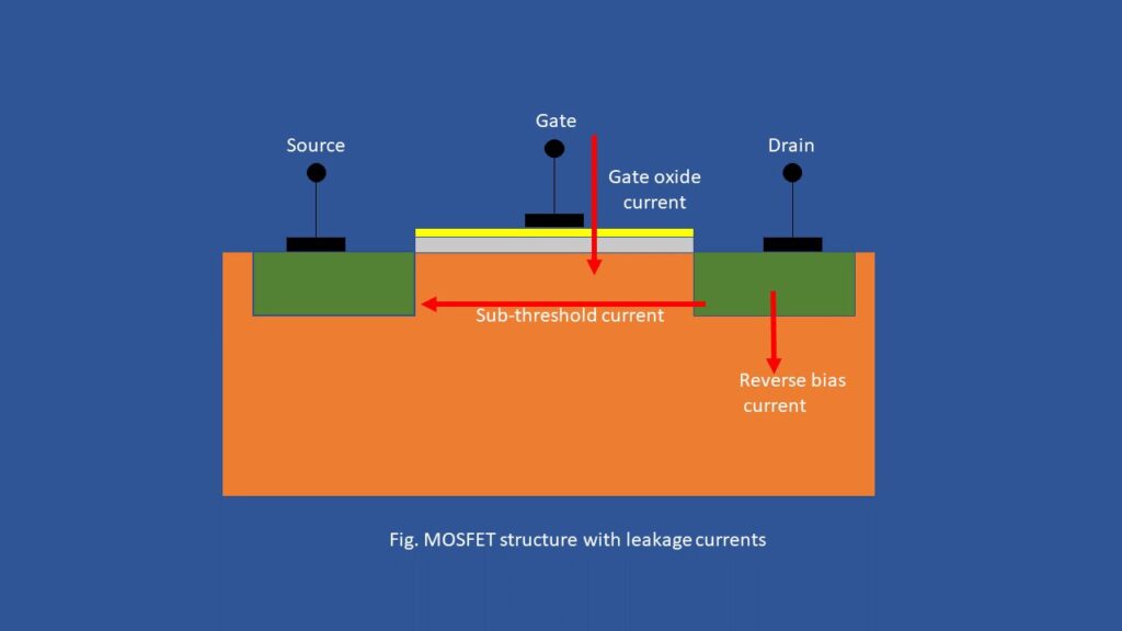
When the circuit is not switching, means no change in input and the clock is also not applying to the circuit, under the presence of a power supply. During this period, some power consumption happens by the circuit. This is known as static power dissipation. The reason for the static power dissipation is due to various leakage currents in the MOS transistors. The following list is the leakage currents in the MOSFETs:
- Sub-thresholds conduction –when Vgs<=Vth, leakage current flows from drain to source.
- Reverse bias pn junction – In NMOS, the drain is N-type and the bulk is P-type. So drain is at a higher potential than bulk. Due to this some leakage current flows from the drain to the bulk.
- Gate tunneling – Due to the gate thickness, some leakage current flows from the gate to the bulk.
Dynamic power dissipation
When the circuit is switching from logic 0 to 1 or logic 1 to 0, it consumes power to charge and discharge the load capacitors in the circuit. Dynamic power dissipation happens for two reasons. They are:
- Switching power
- Short circuit power
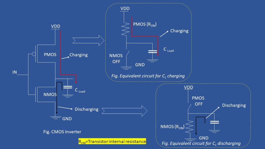
Switching power
When the circuit is switching from logic 0 to logic 1 then power gets drawn from VDD which goes through the PMOS and charges the load capacitor along with other parasitic capacitors. Switching power depends on how often the load capacitor is getting charged and discharged
Pswitch = α.f.CLoad.Vdd2
Where,
α = switching activity
f = frequency
CLoad = Load capacitance
Vdd = Supply voltage
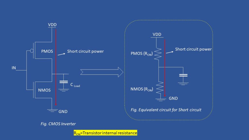
Short circuit power
Short circuit power is a disastrous condition in CMOS circuits, because when the input of the CMOS circuit is switching (transition) from logic 0 to logic 1 or vise-versa, during this transition some period of time both PMOS and NMOS transistors gets turned ON at the same time. Due to this a direct path (low impedance path) can be formed from VDD to GND. Short circuit power is directly proportional to the transition times. Hence, if the transition time is more then short circuit power also more and vise-versa. Following diagram gives you a basic idea of short circuit power.
Pshort circuit = tsc.Vdd.Ipeak
Where,
tsc = transition time
Vdd = Supply voltage
Ipeak = Peak current

hi sir,
could you please provide the info of UPF file
Thank you for comment. Harish we are working on UPF file. Will upload as soon as possible.
Please provide the electromigrition info and low power design techniqued(clock gating, multi voltage design, multi -VT design, power gating)
And low power design cells like level shifters, power switches, isolation cells,retention cells
We appreciate your interest in our content. We’re always looking to provide valuable information to our readers. The topics you’ve mentioned are excellent suggestions, and we’ll definitely consider them for future articles.
Please stay tuned for upcoming content on these topics. In the meantime, if you have any more questions or if there’s anything else you’d like to learn about VLSI or related subjects, please don’t hesitate to ask. Your input is invaluable to us, and we’re here to help you with your interests in VLSI. Thank you for being a part of our community!
Hi there, just became alert to your blog through Google,
and found that it’s truly informative. I’m going to watch out for brussels.
I’ll appreciate if you continue this in future. Numerous people will be benefited from your
writing. Cheers!
Your comment made my day! I’m passionate about VLSI, and it’s rewarding to see that others are finding value in the content. If you have any colleagues or friends interested in VLSI, please share the article with them.
I heard that width of the stripes and top layer width will effect routing .is it true if not can you please elaborate regarding this?
If width of the routes are more, it’s better to route at top layers because those routes which have more width will cause routing congestion. So, that’s why Power routes are routed at top layers and below the power routes Clock routes and at bottom layer signal routes are routed.
power route widths are more, clock routes widths are lesser than power routes and finally signal nets are smaller than both power and clock routes.
Thank you
how we identify design is multi voltage ?
You have verify upf file, there you can find how many power domains are there in the design. If design don’t have any upf file as input. That means design have only one power domain.
Thank you
What are follow pins for?
Follow pins are nothing but power rails which connects the power vias to power pins of standard cells to delivery the power from the power stripes to standard cells trough the power vias and follow pins
Explain the difference between stacked via and array via
Stacked Vias:
A stacked via is a vertical connection where vias are aligned directly on top of each other across multiple metal layers. This means that each via in the stack connects a layer directly above it to a layer below it.
Array Vias:
An array via consists of multiple vias arranged in a grid-like or array structure, typically used to connect two adjacent metal layers (rather than multiple layers like stacked vias). Instead of a single via, multiple vias are placed side by side, distributing current flow across several via points.
Thanks for sharing your knowledge here…
In powerplan how it calculate timing like setup? And how it works? What if get setup violation after checking powerplan ?
Can you explain better way.
We don’t need to calculate timing at powerplan stage. The timing whatever you are seeing at powerplan stage was from synthesis stage. We have check timing from placement stage…
what is mean by bottom up powerplan and topdown power plan and what is the difference between those two
Bottom-Up: first create power plans for individual blocks. These smaller power plans are then integrated to form the power distribution network at higher levels.
Top-Down: Designers create a global power distribution plan for the entire chip first. The power network is then refined and detailed as the design progresses to lower levels.