
In this post we are going to see some basics
First thing you need to know is Physical Design is not a rocket science. Anyone can learn easily with little effort. Remove the fear in your mind and start learn with excitement
Lets get into the topic
There are 2 main components we need to focus in Physical design
1) Resistor
2) Capacitor
Resistor
Resistor is a passive 2 terminal electronic component which opposes the flow of electrons. Resistance is measured in Ohms
symbol of a resistor:
![]()
According to ohm’s law to find resistance
R= V/I
Here
R = Resistor
V = Voltage
I = Current
Resistivity
It is the measure of the ability of a material to oppose the flow of current.
Formula to find Resistivity of conductors for uniform cross section
ρ = RA/I
Here
ρ = Resistivity
R = Resistance
a = cross sectional area of the conductor
l = length of the conductor
Capacitor
A capacitor is a passive 2 terminal electronic component which stores energy in the form of electrostatic energy. It is measured in Farads
it consists of 2 conducting plates separted by a dielectric (insulating material)
Symbol of capacitor
![]()
Formula to find capacitance is
C = εr ε0 A/d
Here
c = capacitance
ε0 = permittivity of free space
εr = permittivity of dielectric medium
d = distance between the plates
A = area of the 2 conducting plates
Types of capacitances:
- Area capacitance
- Fringing capacitance
- Coupling capacitance
Note: Capacitor plays a major role in physical design.The relation between capacitor & physical design engineer are like wife & husband no matter how many fights they got into….at the end of the day they won’t live without each other
Area capacitance
Area capacitance is formed among the metal interconnects and base layer. Here, base layer acts as a one conducting plate and metal layer acts as 2nd conducting plate and in between the area is filled by dielectric material. So, there forms some capacitance which is consider as area capacitance.
Based on the above statement, we can say the bottom metal interconnect layer carries more capacitance compared to top metal interconnect layers. Because we know that gap between the conducting plates leads to less capacitance.
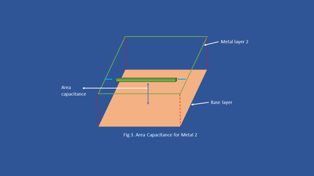
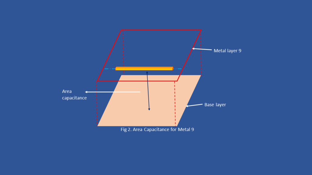
If you see the above example, Metal 2 is near to base layer compared to Metal 9. So, Metal 2 will have more area capacitance compared to Metal 9.
Formula of Area capacitance:
Carea= (∈ L W)/h
∈ = permittivity
L = Length of the wire
W = Width of the wire
h = height
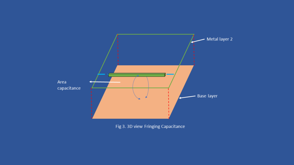
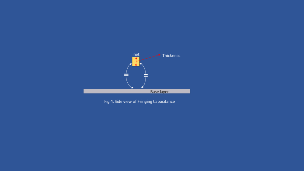
Fringing capacitance
Fringing capacitance another name is side wall capacitance.It is also similar to area capacitance but only difference is the capacitance can be considered from base to sides of the metal layers. You can see the following image for better understanding.
Formula for Fringing capacitance:
Cfring= 2 * (∈ L T)/h
∈ = permittivity
L = Length of the wire
T = Thickness of the wire
h = height
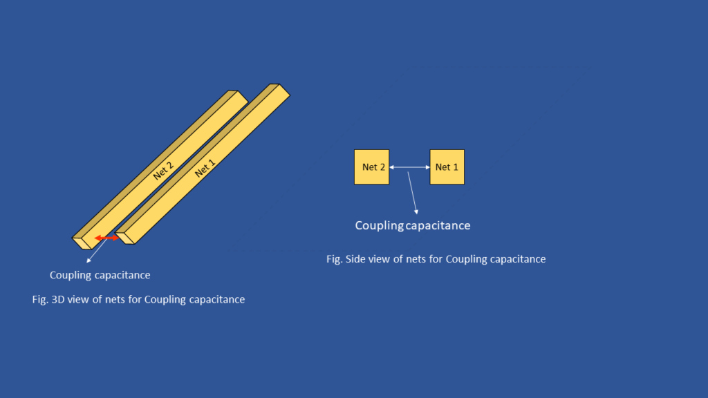
Coupling capacitance
Coupling capacitance is formed in between the nets in the same layer. If 2 nets are running parallel for long distance in the same metal layer then coupling capacitance will be formed. Coupling capacitance should be less as much as possible because it is reason for the crosstalk in the design. Following image shows an example for the coupling capacitance.
Formula for Coupling capacitance
Ccc= (∈ A)/d = (∈ LT)/d
∈ = permittivity
L = Length of the wire
T = Thickness of the wire
d = distance
Propagation Delay
Propagation Delay is nothing but the time takes for the input signal to reach its output
The reason for this delay is due to internal resistance and capacitances
For example if we turn on the light it won’t glow immediately it takes some time the input we given to reach its output but generally we didn’t notice that delay beacause the delay is very very less
Lets see more detail how the delay happens
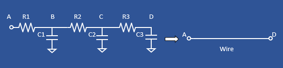
The above circuit represents a conductor (wire) which consists of internal capacitances and resistance.Let us assume it as a wire, point A is the starting point where we give input similarly, point D is the ending point where we take output. If we applied input it goes through R1 and C1 before going to R2 it takes some time to charge at C1 and the process goes on until the given input is reaches to output (point D)
Here we have to focus on two things mainly first one is the length of the wire increases the number of internal resistances and capacitances increases it takes more time to reach output because of capacitors charging and discharging. The second thing is because of more resistances the input which we have given might not be exact when it reaches to output due to loss in travelling.
So here we got to know that issues what we faced whie using long wires the solution for this is adding buffers in between the long wires. Here the buffer acts as repeater and used to reproduce the input signal.
Elmore delay
Elmore proposed an approximate way of calculating the delay of a network consists of resistors & capacitors (Distributed Networks)
Following this we can find out the delay of a wire by dividing the wire into smaller segments without loosing much of accuracy for a length of wire L, if r and c are resistance per unit length and capacitance per unit length Elmore delay of the wire is
rcL2
Here is the example for Elmore delay have a look
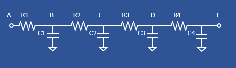
The delay from
From A to B:
R1(C1+C2+C3+C4)
From A to C
R1(C1+C2+C3+C4) + R2(C2+C3+C4)
From A to D
R1(C1+C2+C3+C4) + R2(C2+C3+C4) + R3(C3+C4)
From A to E
R1(C1+C2+C3+C4) + R2(C2+C3+C4) + R3(C3+C4) +R4C4
From B to C
R2(C2+C3+C4)
From C to E
R3(C3+C4) + R4C4
By using this Elmore delay we are going to find delays in the upcoming examples
In the next part of basics we will see about MOSFET
For next part of basics go through this link below

Thank you so much all the contents in each topic are explained very well.. thank you for helping people to learn PD
Thank you
Please update other topics too
We are working, soon we post all the content…
Hi sir here Nagendra can u please give some clarity about how can we decide block shape and what factors we can consider for. That
Usually, shape of the block is square, rectangle or rectilinear. Based on the hierarchy, logic complexity shape cab be decided by the top level engineer.
CMOS Modelling and BASIC CMOS working that also please cover it really help
In the next part of basics we will try to cover those topics
point A to point E is good but in the figure it may had mistaken..in propagation delay.
Thanks for your review, I will change the figure very soon. I hope you like the content.
Just landed on your webpage….very good content with precise explanation….appreciable efforts, Thank you & keep going!