
What is CTS
CTS (Clock Tree Synthesis) is the process of connecting the clock from clock port to the clock pin of sequential cells in the design by maintaining minimum insertion delay and balancing the skew between the cells using clock inverters and clock buffers. Dont worry about the terms insertion delay,skew. You will get to know about it by the end of this post.
Usually clock nets are also comes under High Fanout Nets, but these nets are excluded in High Fanout Net Synthesis (During HFNS, clock nets must have to set don’t touch constraint).Because like normal net we can’t do routing, clock consumes 30% to 40% power in the chip, and clock nets are more prone to EM effect. So, clock nets need some special criteria to do routing (like building clock tree) and have to add ICG cells to control the clock dynamic power. Skew and insertion delay are also having to manage, for that clock buffers and clock inverters are used while building the clock tree.
And one more thing is depending on the clock frequency and design complexity, for some designs building clock tree is easy and for some designs building clock tree is difficult to build. But remember clock tree must and should have to build for every design.
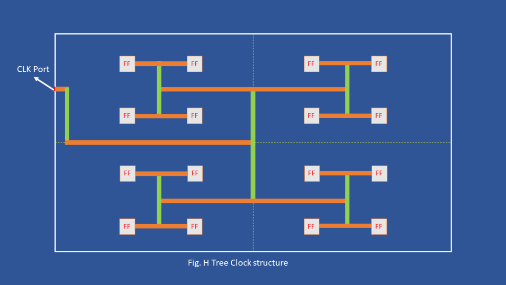
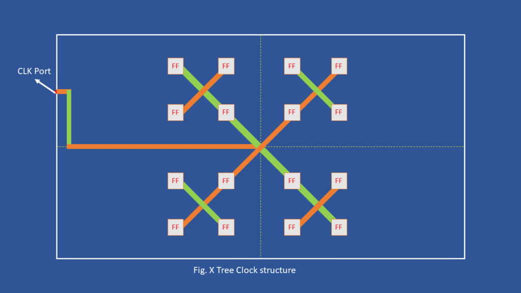
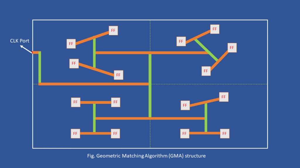
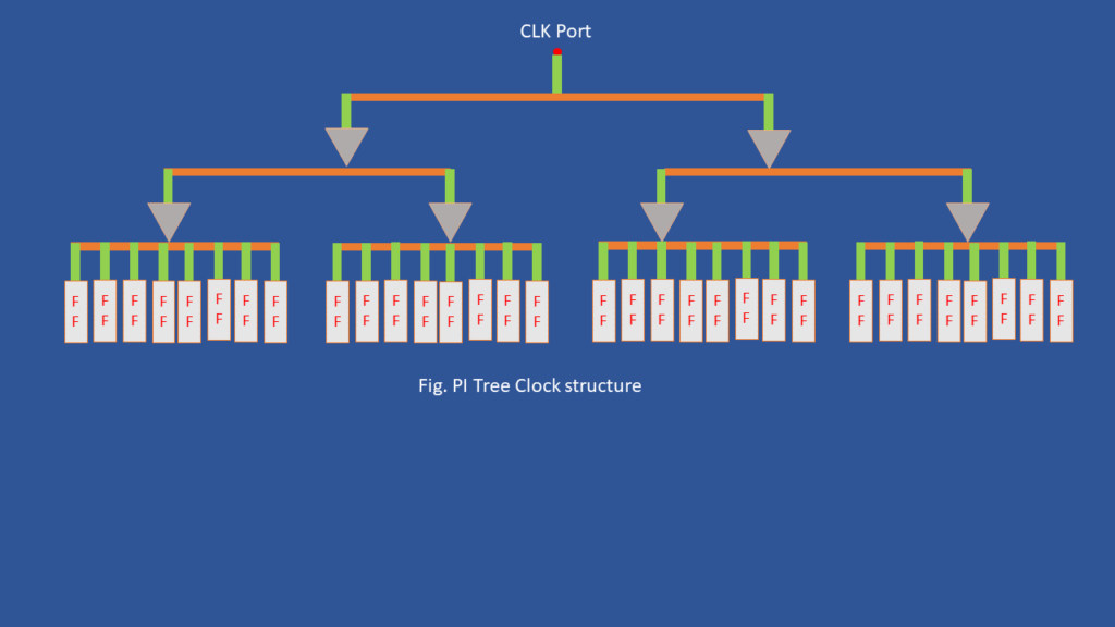
Types of clock tree structures
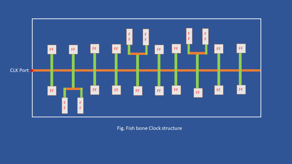
Different structures are available to build clock tree to maintain minimum insertion delay and balance the skew. Few clock tree structures are demonstrated below.
- H – Tree structure
- X – Tree structure
- Geometric Matching Algorithm (GMA)
- Pi Tree structure
- Fish bone
CTS INPUTS
- Placement DB :
- Netlist after placement
- LEF and Tech LEF files
- Placement DEF file
- MMMC file :
- LIB files
- QRC Tech files
- SDC
- UPF file (Only if the design have multiple power domains)
- CTS spec file
CTS Spec file
CTS spec file contains the information like NDR rules,clock buffers and clock inverters, skew and latency targets, leaf nets and trunk nets max and min transistion targets, etc…
Checklist before CTS
- Placement – Completed
- Power ground nets – Pre Routed
- Estimated Congestion – acceptable
- Estimated Timing – acceptable (~ 0ns slack)
- Estimated Max Tran/Cap – No violations
- High Fanout Nets
- Logical / physical library should have special clock cells (clkBuf or clkInv)
CTS Goals
- Minimum Skew
- Minimum Insertion delay
- Complete the clock tree with no DRV (Tran, cap and fanout) violations.
- No timing violations (Setup and Hold)
Clock latency
Latency means the amount of time taken by the clock to reach from clock source to clock pin of sequential element. There are two latency components, source latency and network latency. Source latency is from clock source point to clock definition point and network latency is from clock definition point to the clock pin of the sequential element. Reason for this delay is parasitic capacitance and resistance of nets. Below image show an example of the latency.

Insertion delay
Insertion delay is the delay takes by the clock to travel from clock port to the clock pin of sequential element. It is the delay that added by the clock buffers or inverters in the clock path.So, basically insertion delay is nothing but latency, after CTS latency can be termed as insertion delay. Latency is the virtual delay which gives as a target delay to the tool to achieve. And insertion delay is the real delay that achieved by the tool after building the clock tree.
Skew
Skew is one of the important things to build clock tree in design. It is the difference in arrival times of clock at different points. In low frequency design skew may not create big problems. But in high frequency designs a small difference in clock arrival times can cause significant problems.Skew effects the both setup and hold times.
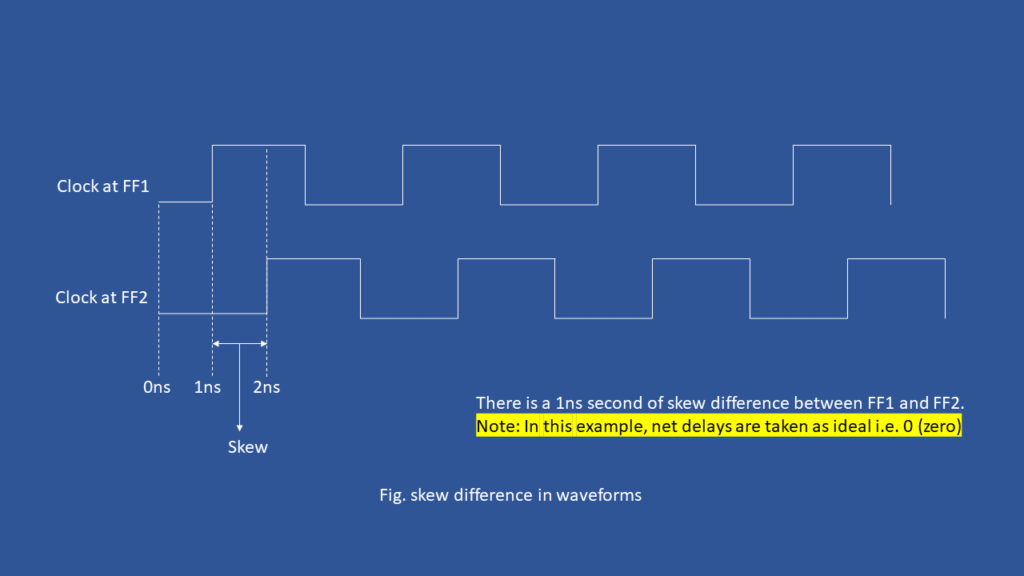
In the above figure, FF1 is placed near to clock port with 1 buffer in the clock path. Similarly, FF2 is placed far away from the clock port with 2 buffers in the clock path. Where, each buffer delay was 1ns then clock will reach late to the FF2 compared to FF1. For FF2, net delays and buffer delays are more compared to FF1 net delays and buffer delay.
Skew can be divided into 2 types:
- Positive skew
- Negative skew
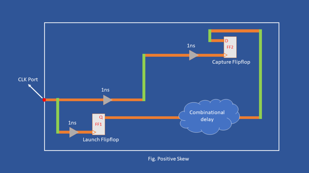
Positive skew
If the capture clock path delay is more compared to the launch clock path delay then it is considered as positive skew. Positive skew improves setup time and degrades the hold time.
Negative skew
If the capture clock path delay is less compared to the launch clock path delay then it is considered as negative skew. Negative skew improves hold time and degrades the setup time.

Types of skew
Based the paths considered to calculate the skew, it can be represented into two types:
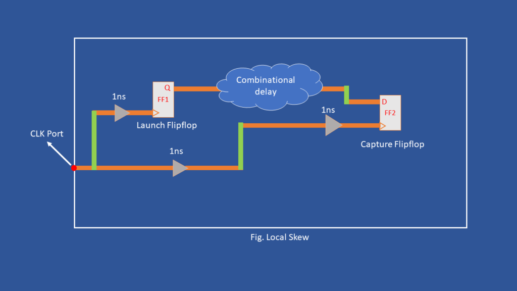
- Local skew
- Global skew
Local skew
If the skew is calculated between the talking flipflops, then it is called as local skew.

Global skew
Global skew is calculated between non-talking flops, it is the difference between the maximum insertion delay (longest clock path in the design) and minimum insertion delay (shortest clock path in the design).
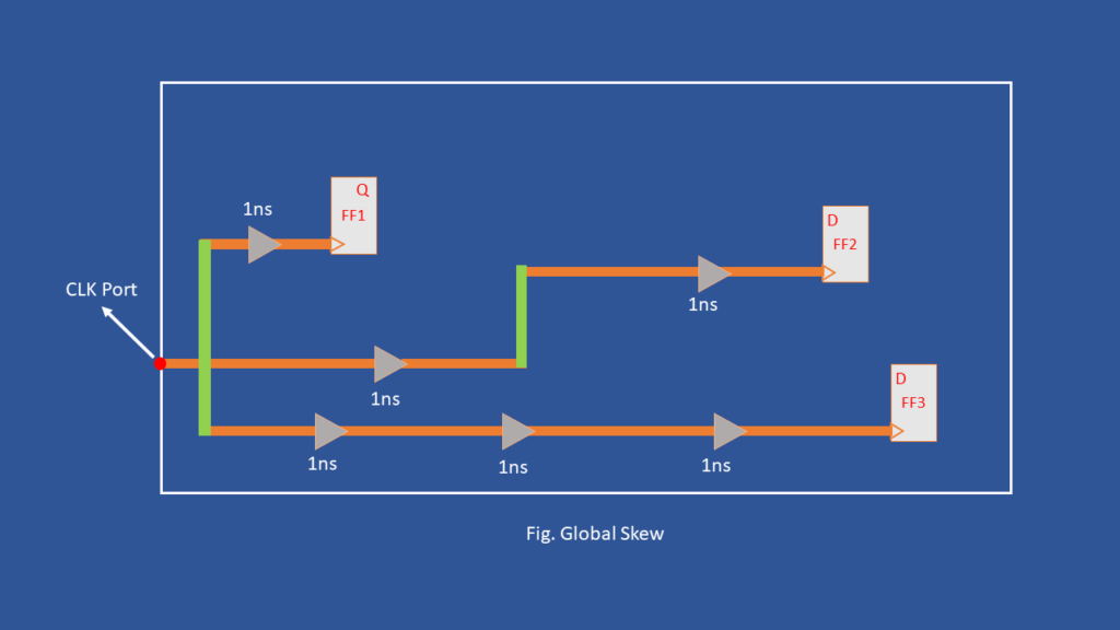
In the above figure,FF1 have shortest clock path and FF3 have longest clock path. So, global skew can be calculated between FF3 and FF1.
Useful skew
As I said skew will improve or degrades setup and hold times. So, skew can be created intentionally to fix the timing violations by adding or deleting the buffers in the clock paths, this adding skew intentionally is termed as useful skew. But before using useful skew make sure that consecutive paths are not getting violate. Because the capture flipflop in path 1 acts as launching flipflop in path 2. So, if you are trying to improve setup in path 1 by adding buffers in capture clock path which will affecttiming in path 2. Similarly, if there is any change in launching clock path in path 2 will affect the timing in path 1, because launch flipflop in path 2 acts as capture flipflop in path 1. So, make sure before using useful skew.
Clock jitter
Consider an ideal clock with 10ns of time period, for this clock, 1st rising edge comes at 0ns and falling edge at 5ns and 2nd rising edge comes at 10ns. Example of ideal clock is shown in below figure. Now, in real world electronic devices never follow ideal conditions there may be some deviations will occur.
Clock jitter means the variation in clock edge arrivals from its ideal position. This variation comes because of noise, interference and thermal effects. The below image shows an example of clock jitter. This jitter will affect the timing of the design. There are two types of clock jitter:
- Deterministic clock jitter – due to crosstalk
- Random clock jitter – due to noise, thermal effects
Deterministic clock jitter can be fixable, by minimizing crosstalk we can avoid, but random clock jitter is unpredictable to avoid random jitter high quality clock source have to use in the design.

In the above figure, there is variation in clock edge which is indicated in orange color. The clock edge is coming either early nor late from its ideal position, so this variation in clock is known as clock jitter.
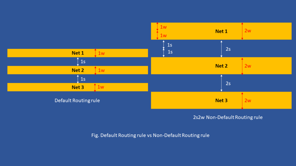
NDR (Non-Default Routing) rule
There are some default routing rules for each and every routing layer like min width, min spacing. Those rules have to follow while doing routing. This default routing rules are coming from foundry (you can find those rules in Tech LEF files). But few nets need some special care compared to normal nets, because those nets are very sensitive to Crosstalk, EM and IR. So, to avoid these issues in nets there may be some changes are required in default routing rules like maintaining extra width, spacing.
So, NDR rules are we can say user specified routing rules. Commonly using NDR rules are “2s2w”, “3s3w”, “2s1w” etc. Here, 2s2w means double spacing and double width, similarly, 3s3w means triple space and triple width.
Why clock nets need NDR rules? Because, once chip is powered ON clock signal continuously switches with very high frequency in clock nets, and those nets are active until the power OFF. Due to this reason there is a high possibility for clock nets to effected by the EM (Electro Migration) & entire chip timing only depends on clock signal, so, clock signal should not affect by any crosstalk or noise. So, extra width has to maintain to avoid EM and extra space have to maintain to avoid crosstalk. The following image shows an example to the Default routing rules vs NDR rules.
Steps in CTS
The clock tree can be builds mainly in 4 steps:
- Clustering
- Balancing
- Routing of clock tree
- Post conditioning
Clustering
During clustering, tool will build only a DRV-aware clock tree and will not balance the clocks. AT the start of this step, tool will print the maximum driver distance and the unit delay for the clock buffer/inverter from a user-provided list or from the library.
Balancing
During this step, tool will balance the design per the skew group constraint. Look for the pattern balancing in the log file. This pattern will repeat multiple times in the log file.
Routing of clock tree
During this step, tool will route all the clock tree nets using a Nanoroute engine.
Post conditioning
This step is run to clean up any minor degradation after the clock routing.
Note: these steps are cadence flow.
CTS Exceptions
While building the clock tree few cells or paths need to manipulate to get better optimized of clock tree. Those manipulation in clock tree can be done by using CTS exceptions. The following 4 exceptions are the major in CTS:
- Stop pin
- Nonstop pin
- Float pin
- Exclude pin
Stop pin
Stop pin also called as Leaf pin or sink pin. Stop pins are the indication to the tool to stop building clock tree at that pin i.e. end point of the clock tree. Tool builds clock tree from clock port to stop pin, stop pins are the reference to the tool to calculate insertion delay and also for skew balance. By default, clock pins of all sequential elements are considered as stop pins.

Nonstop pin
Nonstop pin also called as through pin. Normally clock tree ends at the stop pins, but there is a scenario that tool have to penetrate trough the stop pin, and have to build the clock tree to all the pins connected to the output of that particular sequential element. The perfect example of the nonstop pin is frequency divider circuit, which is shown in following image

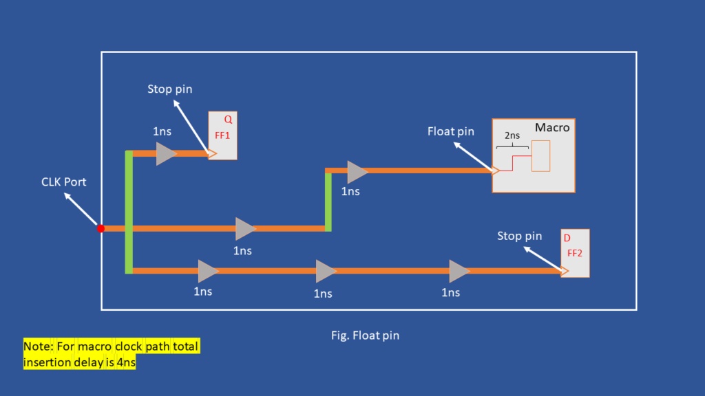
Float pin
Float pin also called as macro modeling. Suppose, if there is some insertion delay inside of the sequential element which have to consider and balance accordingly while building the clock tree. Example of the float pin have shown in below figure
Exclude pin
Exclude pins are isolates the pins from clock tree even clock is going to that particular pin. Isolates means timing, balancing and optimization are not consider for the clock tree calculations. The example of the exclude pin is shown in following image

Clock tree optimization techniques
While building the clock tree tool following few optimization techniques which are mentioned below:
- Buffering
- Sizing
- Cloning
- Load splitting
- Vt changing
- Instance relocation
- Useful skew
CTS outputs
- Netlist after CTS
- CTS DEF
- Timing reports (setup and hold)
- Skew and Latency reports
Checks after CTS
- Insertion delay (Target have to meet)
- Skew (Target have to meet)
- Routing congestion
- Placement legality
- Signal integrity and crosstalk
- Clock duty cycle
- Clock tree power consumption

Thankyou for PD information.why STA in content protected ? your content is so easy to understand for beginner student. please provide the STA also.
Hi Harish,
We are not yet updated STA.The content will be updated soon
Please post STA content
Hi chandu, we are working on it
Can you explain how cross talk is affecting the clock nets ?
Entire timing of the design depends on clock. If crosstalk is affecting the clock nets, there may see double clocking or triple clocking. Let’s consider there is a crosstalk affect in clock net, like aggressor is in constant low and victim net (clock net) is switching 0 to 1, which will pull the clock transition to 0. Assume the aggressor pulling the clock transition after triggered the flop and falls back to 0 and again rising to 1. Here, again triggering the flop immediately. this is how crosstalk impact.
And also it may increase the insertion delay and clock jitter.
What is the difference between port and pin,?
In the design, we have many cells each cell will have one or more inputs each input considered as pin. And pins which connects the two or more blocks are considered as port.
what about postcts?
During post CTS stage, if CTS requirements(like skew, insertion delay) are not reached, then we do some ECO to meet the requirements…
post a sta concepts sir
I truly appreciate your interest, we are working on left over topics…
what is mean ICG cells?
ICG means Integrated Clock Gating. It is used to block the clock when the flops are in ideal mode. By doing this we can able to reduce clock dynamic power.
Why Content is protected ? I can’t load the images that you have shown..
Hi Bhaskar, we have updated all images. Please check now. Thank you
Content is very helpful, cloud please explain the CTS Optimizations techniques also
Good information